A researcher works with a chip��in a facility on the ����������ý�Ļ���Ʒ campus. (Credit: ����������ý�Ļ���Ʒ College of Engineering and Applied Science)
This month marks a victory for very, very small electronics.��
On Aug. 25, President Joe Biden signed an executive order meant to speed up the start of the in the U.S. The bill, which passed the Senate earlier this summer with a bipartisan vote of 64-33, seeks to funnel $280 billion toward various research and tech programs around the country—including nearly $53 billion in investments to spur the country’s shrinking semiconductor industry.��
Aju Jugessur joined a number of researchers at ����������ý�Ļ���Ʒ who celebrated the bill.
Researcher works in the clean room at the COSINC facility on the ����������ý�Ļ���Ʒ campus. (Credit: Cu Boulder College of Engineering and Applied Science)
Researcher looks through a microscope at COSINC. (Credit: ����������ý�Ļ���Ʒ College of Engineering and Applied Science)

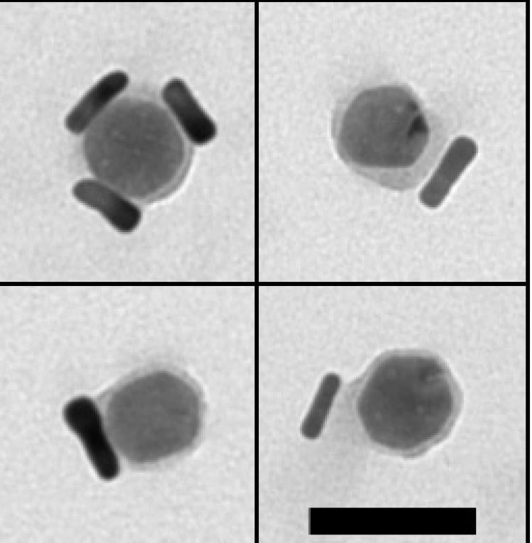
Microscope image of nanostructures designed by Won Park and his colleagues at CU Anschutz binding to cancer cells in the lab. (Credit: Won Park)
He oversees a facility on campus called the Colorado Shared Instrumentation in Nanofabrication and Characterization (COSINC). Here, researchers use state-of-the art tools to design incredibly small electronic devices—some features measuring just 10 nanometers in size, or less than a millionth of an inch. What impacts the CHIPS and Science Act will have on ����������ý�Ļ���Ʒ and Colorado are still unclear. But Jugessur noted that it brings new attention to a critically important, but often overlooked, class of materials called semiconductors. Today, semiconductor devices are everywhere, powering the chips inside your smart phone, car, laptop and even thermostat.��
But their supply in the U.S. has grown increasingly shaky as factories have shifted overseas, and supply-chain disruptions have driven the cost of semiconductors sky-high.
“The minute you get up, almost everything you touch uses semiconductor chips,” Jugessur said. “We learned the hard way during this pandemic that we cannot rely on other countries to provide these chips. We have to make our own.”
The engineer isn’t only interested in the electronics of today. He’s also focused on enabling research on the technologies that consumers will use 20 or 30 years from now.
At COSINC, part of the College of Engineering and Applied Science, researchers design new kinds of incredibly-small electronics—from tiny sensors that could squeeze on top of a grain of salt to devices that may be able to seek out and destroy tumor cells hiding in the body. Still more researchers will use the facility to develop quantum technologies that can harness light in never-before-seen ways.��
“Ever since nanotechnology emerged several decades ago, it has become something we as a society rely on for so many things,” said Won Park, professor of electrical computer and energy engineering who has worked extensively at COSINC.
Training grounds
To show just how much the world depends on nanotechnology, Jugessur holds up his iPhone 13. This pocket-sized device, he said, contains roughly 15 billion semiconductor transistors, a key feature of computer chips.
“I basically live in my iPhone. I have my calendar. I have my email. I can control my home security features from here,” said Jugessur, a physicist and electrical engineer by training. “All that is thanks to semiconductors.”
Semiconductors are a wide class of materials that include germanium and the silicon that gives Silicon Valley its name. They exist in a kind of middle zone of electronics—mixing the properties of conductors, such as copper wires, and insulators, such as rubber.
Currently, facilities in the United States produce about 12% of the semiconductors made every year world-wide. This year’s CHIPS and Science Act is an attempt to address that shortfall. Large portions of the bill’s funding will likely go to businesses in the U.S. that fabricate transistors like those in Jugessur’s smart phone. But the act also authorizes new funding for��basic research through agencies like the U.S. National Science Foundation and��gives NASA the official go-ahead to pursue its Artemis program to return to the moon. ��
If that funding is approved, researchers across ����������ý�Ļ���Ʒ, including at COSINC, may be able to apply for new grants to tap into the windfall.
Jugessur noted that at COSINC, researchers and students gain experience with some of the same tools and processes that the nation’s semiconductor plants employ. Students, for example, can try their hands at a process called photolithography. In this multi-step technique, engineers use lasers, solvents and polymers, or plastics, among other tools to carve thin structures on wafers of semiconductor materials into precise shapes.
The facility’s new $8.5 million clean room is scheduled to open in October.
“If you're not training the next generation of people, in our case, students, to work in this area, the semiconductor industry in the U.S. won’t be able to compete,” Jugessur said.
Zapping tumors
Park’s research shows the promise of the nano domain.��
He uses machines at COSINC to design tiny electronics that take a deep dive into the equally tiny world within the human body. In one project, for example, Park and his colleagues have like burrs sticking on pants after a hike. If you hit the devices with the right color of light, they begin to heat up, potentially destroying the tumors in the process. One day, doctors could potentially treat bladder cancer by introducing these nanodevices into a patient’s bladder��through a urinary catheter.��
“With these devices, you wouldn’t need to have surgery to remove bladder cancer,” Park said. “You could potentially do this treatment in an outpatient clinic.”
The project is a collaboration with researchers at the CU Anschutz Medical Campus. The team has tried out this nano-sized approach to medicine on tumors cells in a lab but hasn’t yet tested it in humans.��
Park added that COSINC is an indispensable part of campus. You can’t make the technology of the future, he said, without getting small.
“Without COSINC, I wouldn’t have a research program,” he said. “Being able to fabricate structures in these nanoscale dimensions is absolutely essential in today’s world."


